- 您现在的位置:买卖IC网 > Sheet目录337 > LHF00L28 (Sharp Microelectronics)IC FLASH 16MBIT 70NS 48TSOP
�� �
�
�LHF00L28�
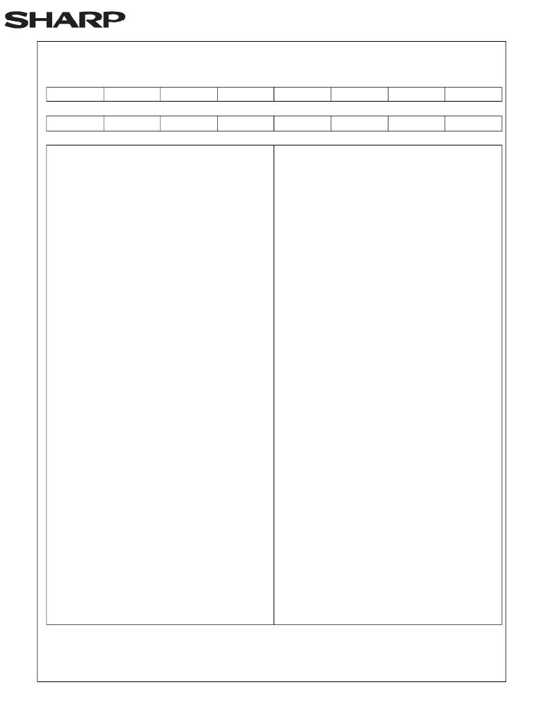
�Table� 8.� Status� Register� Definition�
�13�
�R�
�15�
�WSMS�
�7�
�R�
�14�
�BESS�
�6�
�R�
�13�
�BEFCES�
�5�
�R�
�12�
�POPS�
�4�
�R�
�11�
�WPACCS�
�3�
�R�
�10�
�PSS�
�2�
�R�
�9�
�DPS�
�1�
�R�
�8�
�R�
�0�
�SR.15� -� SR.8� =� RESERVED� FOR� FUTURE�
�ENHANCEMENTS� (R)�
�SR.7� =� WRITE� STATE� MACHINE� STATUS� (WSMS)�
�1� =� Ready�
�0� =� Busy�
�SR.6� =� BLOCK� ERASE� SUSPEND� STATUS� (BESS)�
�1� =� Block� Erase� Suspended�
�0� =� Block� Erase� in� Progress/Completed�
�SR.5� =� BLOCK� ERASE� AND� FULL� CHIP� ERASE�
�STATUS� (BEFCES)�
�1� =� Error� in� Block� Erase� or� Full� Chip� Erase�
�NOTES:�
�Status� Register� indicates� the� status� of� the� WSM� (Write� State�
�Machine).�
�Check� SR.7� or� RY/BY#� to� determine� block� erase,� full� chip�
�erase,� program� or� OTP� program� completion.� SR.6� -� SR.1� are�
�invalid� while� SR.7="0".�
�If� both� SR.5� and� SR.4� are� "1"s� after� a� block� erase,� full� chip�
�erase,� program,� set/clear� block� lock� bit,� set� block� lock-down�
�bit� attempt,� an� improper� command� sequence� was� entered.�
�0� =� Successful� Block� Erase� or� Full� Chip� Erase�
�SR.3� does� not� provide� a� continuous� indication� of� WP#/ACC�
�SR.4� =� PROGRAM� AND�
�OTP� PROGRAM� STATUS� (POPS)�
�1� =� Error� in� Program� or� OTP� Program�
�0� =� Successful� Program� or� OTP� Program�
�SR.3� =� WP#/ACC� STATUS� (WPACCS)�
�1� =� V� CC� +0.4V� <� WP#/ACC� <� 11.7V� Detect,�
�Operation� Abort�
�0� =� WP#/ACC� OK�
�level.� The� WSM� interrogates� and� indicates� the� WP#/ACC�
�level� only� after� Block� Erase,� Full� Chip� Erase,� Program� or�
�OTP� Program� command� sequences.� SR.3� is� not� guaranteed� to�
�report� accurate� feedback� when� WP#/ACC� ≠� V� ACCH� .�
�SR.1� does� not� provide� a� continuous� indication� of� block� lock�
�bit.� The� WSM� interrogates� the� block� lock� bit� only� after� Block�
�Erase,� Full� Chip� Erase,� Program� or� OTP� Program� command�
�sequences.� It� informs� the� system,� depending� on� the� attempted�
�operation,� if� the� block� lock� bit� is� set.� Reading� the� block� lock�
�configuration� codes� after� writing� the� Read� Identifier� Codes/�
�OTP� command� indicates� block� lock� bit� status.�
�SR.2� =� PROGRAM� SUSPEND�
�STATUS� (PSS)�
�1� =� Program� Suspended�
�0� =� Program� in� Progress/Completed�
�SR.15� -� SR.8� and� SR.0� are� reserved� for� future� use� and� should�
�be� masked� out� when� polling� the� status� register.�
�SR.1� =� DEVICE� PROTECT� STATUS� (DPS)�
�1� =� Erase� or� Program� Attempted� on� a�
�Locked� Block,� Operation� Abort�
�0� =� Unlocked�
�SR.0� =� RESERVED� FOR� FUTURE� ENHANCEMENTS�
�(R)�
�Rev.� 2.45�
�发布紧急采购,3分钟左右您将得到回复。
相关PDF资料
LPM409 CHASSIS
STNRD 4SLOT CHASSIS W/INPUT LEAD
LS15RB1201J04
POE SPLITTER 10.8W 12V @0.9A
LT1932ES6#TRMPBF
IC LED DRIVR WHITE BCKLGT TSOT-6
LT1937ES5#TRMPBF
IC LED DRIVR WHITE BCKLGT TSOT-5
LT3003EMSE#TRPBF
IC LED DRIVER BALLASTER 10-MSOP
LT3465AES6#TRMPBF
IC LED DRIVR WHITE BCKLGT TSOT-6
LT3466EDD-1#PBF
IC LED DRIVR WHITE BCKLGT 10-DFN
LT3466EDD#PBF
IC LED DRIVR WHITE BCKLGT 10-DFN
相关代理商/技术参数
LHF00L29
功能描述:闪存 16Mb 3VBottom Boot Single Supply RoHS:否 制造商:ON Semiconductor 数据总线宽度:1 bit 存储类型:Flash 存储容量:2 MB 结构:256 K x 8 定时类型: 接口类型:SPI 访问时间: 电源电压-最大:3.6 V 电源电压-最小:2.3 V 最大工作电流:15 mA 工作温度:- 40 C to + 85 C 安装风格:SMD/SMT 封装 / 箱体: 封装:Reel
LHF00L30
功能描述:闪存 16Mb 3VTop Boot Dual Supply RoHS:否 制造商:ON Semiconductor 数据总线宽度:1 bit 存储类型:Flash 存储容量:2 MB 结构:256 K x 8 定时类型: 接口类型:SPI 访问时间: 电源电压-最大:3.6 V 电源电压-最小:2.3 V 最大工作电流:15 mA 工作温度:- 40 C to + 85 C 安装风格:SMD/SMT 封装 / 箱体: 封装:Reel
LHF00L31
功能描述:闪存 16Mb 3VBottom Boot Dual Supply RoHS:否 制造商:ON Semiconductor 数据总线宽度:1 bit 存储类型:Flash 存储容量:2 MB 结构:256 K x 8 定时类型: 接口类型:SPI 访问时间: 电源电压-最大:3.6 V 电源电压-最小:2.3 V 最大工作电流:15 mA 工作温度:- 40 C to + 85 C 安装风格:SMD/SMT 封装 / 箱体: 封装:Reel
LHF00L47
制造商:Sharp Microelectronics Corporation 功能描述:8MB NOR FLASH FOR CISCO ROHS COMPLIANT - Trays
LHF-03-SA2-X02
制造商:Adam Technologies Inc 功能描述:3 Position Board Mount Header 5 mm Pitch
LHF-03-SB1-V2-EU
制造商:Adam Technologies Inc 功能描述:
LHF04C01
制造商:SHARP 制造商全称:Sharp Electrionic Components 功能描述:4M Flash File Memory
LHF04C10
制造商:SHARP 制造商全称:Sharp Electrionic Components 功能描述:4Mbit Flash Memory